» Semiconductor > Semiconductor Material Marking Equipment > Semiconductor Wafer Marking Semiconductor Wafer Marking
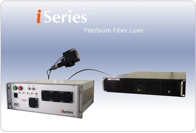
Wafer marking is important in the raw material phase to eliminate fault analysis. Sometimes after the wafer is made it can have a defect and there is no way of tracking where the defect came from. Laser marking provides the ability to trace the wafer's origins, eliminating these problems. The laser mark on the wafer occurs before the wafer has been diced and processed. Utilizing laser marking, as opposed to ink marking, is the best solution because it provides a mark that is permanent, readable, and high quality enough to meet even the most stringent requirements. Wafer marking can be applied to both the semiconductor and solar panel industries. As wafers move to components the i-Series Fiber Laser Marking Kit is a safe method for wafer marking. The thinnest wafer will not be harmed during the manufacturing process guaranteeing a low-maintenance, fault-free operation in clean-room environments.
|
|||||||||||||||
Semiconductor
Semiconductor Dicing and Scribing Equipment
Semiconductor Material Marking Equipment
Semiconductor Wafer Marking
Semiconductor Chip Marking
IC Chip Failure Analysis
Coating Removal
 Member of Semiconductor Equipment and Materials International |
Need a Laser Solution:
Call Us at: Highlighted Application:
Contact Us:
| ||||||||||||||
