» Semiconductor > IC Chip Failure Analysis FiberTower™ DFAS - IC Chip Package Failure Analysis System
The process that most failure analysis labs use on a routine basis, is chemical and mechanical etching. The DFAS uses our laser technology to allow an operator to remove individual layers of the mold compound all the way through the lead frames to the substrate. Unlike the uncontrollable chemical etch process, the DFAS Decap process is 100% controllable by the operator through a Graphic User Interface (GUI). The operator can remove the entire compound, individual layers, or sections of the mold compound (operator defined) ranging from the entire sample to just one wire. The DFAS can import images from a variety of testing processes such as C-SAM, SEM, SAM and X-RAY to show the operator exactly the area of concern within the sample. The DFAS Image Patterning software allows for unparalleled protection and precise removal in and around sensitive components. DFAS eliminates the majority of cost, danger, as well as long term health hazards associated with the use chemicals, all with a process of unmatched safety and accuracy. Benefits of Laser Application
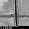
Cross SectioningCross-sectioning is another process commonly used in failure analysis. Until the DFAS was introduced, this process was normally done with a diamond saw. The diamond saw process is very slow and requires many more times additional polishing due to a large stand off required from the cut, and still does not guarantee that the sample will not be damaged. The DFAS utilizes our patented laser cross-sectioning process to provide an extremely accurate dissection without damaging the sample. The DFAS allows the operator to import images from a variety of testing processes such as C-SAM, SEM, SAM and even X-RAY to show the operator exactly were the area of concern is within the sample. Once the area of concern is defined, the operator can utilize the Graphic User Interface (GUI) to define the cross-section. With a beam width of less than 25 μm the system can even cross-section a solder ball. In addition, harvesting of the die or other individual components is now practical. Material CharacterizationThe DFAS incorporates the latest laser spectrometry technology to provide a detailed report of all the materials as they are being processed. The operator can choose the Characterization feature in the software, which enables an array of sensors to gather data as a process is running. For example, if the Characterization feature is utilized with the Decap process, the latest laser spectrometry technology provides enough data to not only tell the operator what is in the compound (using a database of stored mold compounds) but determine if the compound is the same that was ordered from the supplier. This feature is so accurate that inconsistencies within the compound (flow settlement, contaminants) can also be plotted and reported. A report will then be generated detailing the exact characteristics of the mold compound.
|
|||||||
Semiconductor
Semiconductor Dicing and Scribing Equipment
Semiconductor Material Marking Equipment
IC Chip Failure Analysis
Coating Removal
 Member of Semiconductor Equipment and Materials International |
Need a Laser Solution:
Call Us at: Highlighted Application:
Contact Us:
|