» Semiconductor > Semiconductor Dicing and Scribing Equipment > Silicon Wafer Dicing - BlackStar SW300

Silicon Wafer Dicing - BlackStar SW300

silicon wafer dicing laser

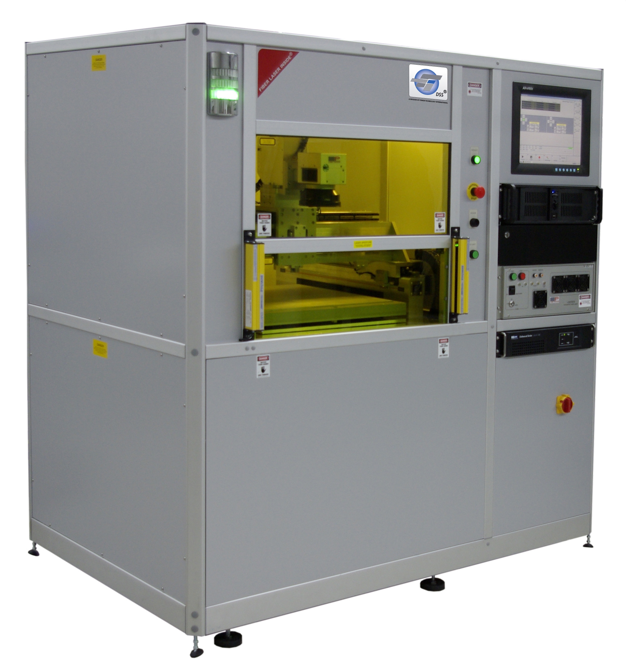
BLACKSTAR™ is a Wafer Dicing System utilizing Fantom Width Laser Dicing Technology® (FWLDT®) invented and patented by Fonon Technology and modified to accommodate the requirements of a silicon wafer singulation process without affecting the existent dicing method, processes or procedures.

Wafers have the highest value at the dicing stage and the primary focus of a BlackStar™ is to increase the number of dies, yield per wafer, and to maximize throughput while minimizing the HAZ specifically for “power hungry” RF micro devices and low-K wafer substrates.
System is applicable for dicing of assorted semiconductor materials such as silicon (Si), gallium arsenide (GaAs), germanium (Ge), indium phosphide (InP), silicon carbide (SiC), gallium nitride (GaN), gallium phosphide (GaP), other compound materials, as well as low-k and multi-layer composite materials.

BlackStar™ is an alternative to mechanical saws too damaging and costly for cutting of thin delicate silicon, low-K and complex material wafers.

Parameter Value
Material Low-K
Street width Thickness dependent
HAZ 0
# of passes required 1
Micro Cracks None
Chipping None
Edge strength Excellent
Clean Room Compatibility Class 1000 or 10000
Water Cooling None

LASER

  • Proprietary Type 

WAFER

  • Wafer thickness - 50µ to 700µ.
  • Wafer size - 12" max.
  • Frame: Standard types (8” or 12")
  • Holding tape: standard low tack

VISION SYSTEM

  • Two-level Magnification 
  • Optical zoom
  • Type: Pattern Recognition with
  • Automatic alignment

MOTION SYSTEM

  • 4 axis direct drive servo platform.
  • Working area 500 x 500 mm
  • Maximum axis speed 500 mm/s


Applications Search:

Total Matching Applications: 138,  Displaying 1 - 3.  
Next 3 Applications >>


Application #105
Process: Ceramic Marking
Material: Ceramics

Application #109
Process: Ceramic Marking
Material: Ceramics

Application #131
Process: Glass Panel Dicing
Material: Glass Panels
Total Matching Applications: 138,  Displaying 1 - 3.  
Next 3 Applications >>


Fonon DSS | Laser Marking & Engraving | Flat Panel Display | Semiconductor | Applications | Employment | About | Contact Us | Site Map

Copyright © 2025 Fonon Display and Semiconductor Systems, LLC


Member of Semiconductor Equipment and Materials International


Need a Laser Solution:


Contact an Expert
Request a Quote
Application Request

Call Us at:
407-804-1000

Highlighted Application:


Application #164
Process: Silicon Wafer Dicing
Material: Semiconductor Wafers


Contact Us:

marking laser Mailing List:
Sign up to recieve news and updates from Fonon DSS!

marking laser Email Us:
Contact our staff or request a quote.