» Solar Panel Processing
Solar Panel Processing
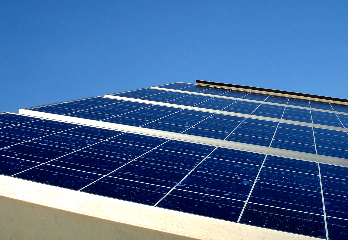
Today, solar power is thought to be the cleanest, most reliable and plentiful energy resource available, though it’s potential has not yet reached fruition. Manufacturers of solar panels most commonly use silicon in processing solar panels, but due to the price increases and supply decreases, the industry is rapidly moving towards thin-film panel processing. Thin-film processing is proven to be notably more cost effective and the supply is abundant and readily available. As thin-film panel processing advances, solar panels are being manufactured at G8 sizes due to the cost efficiency of processing larger panels with minimal yield loss. Using Fiber Lasers, Fonon Display and Semiconductor Systems (Fonon DSS) has developed breakthrough processes and equipment ideal for large solar panel processing. These systems are manufactured from the highest quality components, proven technology and experienced designers and engineers.
System Features Include: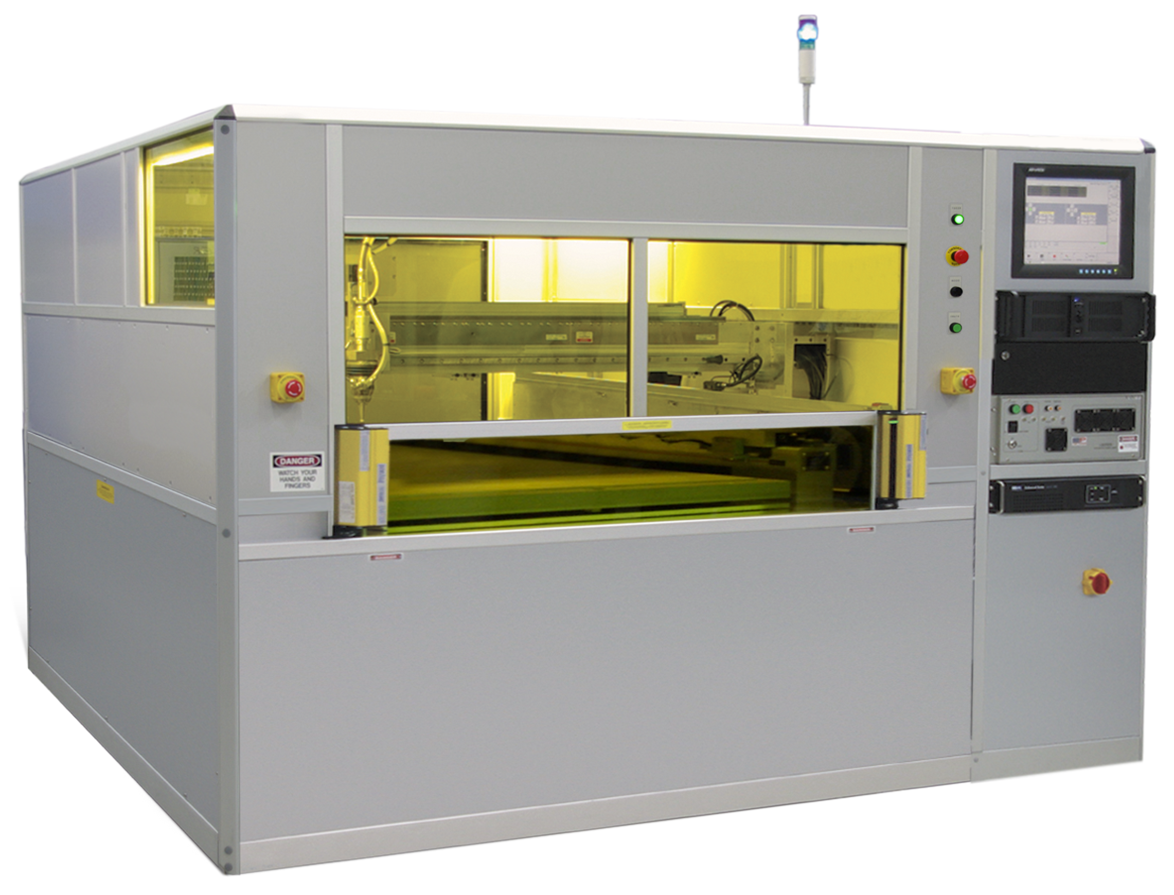
- Beam delivery optics with automatic spot size variability
- Multiple independently positioned beams with X-Y motion systems
- Environmentally friendly process
- High speed linear motors/encoders
- Tolerances of within +/- 0.00075 inches over 8 feet of travel
There are multiple steps involved in the fabrication of solar panels. Currently, the industry is using 1100 x 1300 mm (G5) sized panels but are beginning to utilize 2200 x 2600 mm (G8) size panels. Fonon DSS has recently designed a system, the Solar Star, which can be configured to scribe these large sized panels. The G8 panels are usually divided into approximately 200 individual solar cells produced by various scribing methods. The Solar Star has the ability to maintain cost effectiveness while processing these large panels at extremely fast speeds. Also, narrow scribe lines needed to create a scribe at 2m/s is achieved in a single pass.
 Fonon DSS has the capabilities to optimize our technology for the solar industry. Fonon DSS has proven this technology in the flat panel and semiconductor industries and is now applying the methods for large solar panel manufacturing. Having already sold a number of systems for G3-G5 panels to the solar industry, Fonon DSS is now setting its sights on manufacturing systems for larger panels. Fonon DSS’s continued research and development of Fiber Laser systems will be a major contributor to the advancement of the solar panel processing industry. Combining high beam quality and accuracy, Fonon DSS has developed the industry’s most definitive solar panel marking, scribing and edge deletion methods available on the market.
Fonon DSS, a division of Fonon Technology International, provides state-of-the-art Laser Scribing, Laser Dicing and Fiber Laser marking solutions to customers in the FPD, Semiconductor and Electronics industries throughout the world. Using our industry knowledge of over 15 years, we specialize in the latest generation laser systems, processes and technologies. At Fonon DSS, our dedication to the advancement of laser technology places us at the forefront of the laser revolution. To learn more about Fonon DSS technology and for all product features and benefits, visit www.Fonondss.com or call our office at 407-829-2613.
Fonon DSS | Laser Marking & Engraving | Flat Panel Display | Semiconductor | Applications | Employment | About | Contact Us | Site Map
Copyright © 2026 Fonon Display and Semiconductor Systems, LLC